Electrical and Electronics Principles
TASK 1
Ohm`s Law
It states that current is directly proportional to the voltage across two given points of a conductor.
I α V
Introducing the proportionality constant R,
I=V/R or V=IR

Ohms law I-V Curve
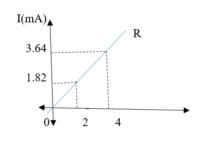
Slope (G) = ∆y∆x = ∆I∆V = 1R = 1.82X10-32 = 0.91mS for 1.1kΩ resistor.
= 2.97X10-38 = 0.37mS for 3.3kΩ resistor.
From the experiment on Kirchoff`s law:

Kirchoff`s Voltage Law
States that the sum of voltages around a closed loop in a circuit is equal to zero. Using the results in the table;
Vs+V1+V2=Vs+V1+V3=0
Considering directionality;
Vs-V1-V2=0
Substituting;
12-7.5-4.8=-0.3, which is close to zero. Inaccurate value due to error in measuring equipment.
Kirchoff`s Current Law
States that sum of current flowing into and out of a node in a circuit is equal to zero. It may also be stated as the current flowing into a junction in a circuit is equal to current leaving the junction.
From the experiment results;
I1=I2+I3
Substituting and considering directionality
0.0034=0.0048-0.0015=0.0033
These values almost balance despite errors in measurement.
Kichoff`s KVL and KCL laws still hold for the above experiment since the acquired results comply with the statement of these laws. Ie sum of voltages in the closed loop is zero and current flowing into a node is equal to those leaving respectively. Some inaccuracy is however experienced due to errors in measuring equipment.

Thevenin`s Theorem
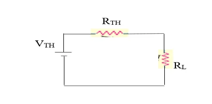
As applied to dc circuits, the theorem states that “current passing through a load across any two points of an active bilateral linear network is given by Voc \\ (Ri+RL) where Voc is voltage when open circuited and Ri is the network`s internal resistance as viewed throu the open circuited terminals, with all current sources replaced by infinite resistance and voltage sources by their internal resistance if any.”
RTH=3.3\\2.2+1= 3.3X2.23.3+2.2+1=2.32kΩ
ETH=2.22.2+3.3X12=4.8V
IL=ETHRTH+RL=4.82.32+0.47=1.72mA
TASK 2
Considering an impedance triangle,
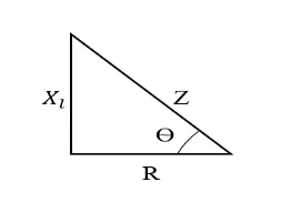
Circuit impedance (Z) is termed as the opposition to current flow and in RL circuit is given by
Z=√(R2+Xl2),
Where R is the resistance in Ohms (Ω) and Xl2 is the inductive reactance in Ohms (Ω).
The inductive reactance,
Xl=ꙍL=2πfL
Where ꙍ=2πf and f=frequency in Hz. L is the inductance Henries (H).
ꙍ=100π implying; Xl=100X801000=8π=25.13Ω
Therefore,
Z=√(1002+25.132)=103.11Ω
The RL circuit is in series hence current is considered to be the same throughout i.e 20mA=0.02A
For a series RL circuit, current across the components is equal. Hence applying Ohms law, voltage across the resistor;
VR=IR
Where I is current across the circuit in Amperes (A) and R is the resistance in Ohms (Ω)
So VR =0.02X100=2V
Voltage across the inductor;
VL=IXl
I is current in Amperes (A) and XL is inductive reactance in Ohms (Ω)
VL=0.02X25.13=0.5V
Phase angle Ѳ=Cos-1 RZ , R representing resistance and Z is the circuit impedance in Ohms (Ω).
Cos-1 100103.11=14.120
b) Since the components are connected in series, current (I) across them is the same 40mA= 0.04A, while the voltages differ.
According to Ohm`s law, voltage across the resistor VR=IR
Where I is current across the circuit in Amperes (A) while R is the resistance in Ohms (Ω)
So VR=0.04X200=8V
Voltage across the capacitor VC=IꙍC=I2πfC
Where I is current across the circuit in Amperes (A), C is the capacitance in Farads (F), f is frequency in Ohms (Ω) and ꙍ = 2πf is angular frequency in rad s-1.
VC=0.04X106100πX22=5.79V
Voltage across the inductor VL=IꙍL=I X 2πfL
Where I is current across the circuit in Amperes (A), L is the inductance in Henries (H), f is frequency in Ohms (Ω) and ꙍ = 2πf is angular frequency in rad s-1.
VL=0.04X100πX801000=1V
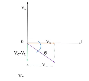
Impedances across the individual elements in the RLC circuit are proportional to voltage since current through the circuit is equal. From the phasor diagram and applying Pythagoras Theorem,
Z=√(R2+(XC-XL)2) or Z=√(R2+(XL- XC)2)
R is the resistance in Ohms (Ω), XC is the capacitive reactance while XL is the inductive reactance in Ohms (Ω)
But XC=1ωC=12πfC=1X1062200π=144.69 Ω
XL=ꙍL=2πfL=8π=25.13 Ω
Therefore,
Z=√(2002+(144.69-25.13)2)
=233 Ω
Applying Kirchoff`s Voltage Law, VR+VC+VL=V
So V=8+5.79+1=14.79V
Applying Ohm`s law, Supply voltage V=IZ
Where I is the current while Z is the circuit impedance
Therefore;
Current I=VZ=14.79233=0.06A
From the phasor diagram and phase difference, phase angle Ѳ is calculated as follows:
Tan Ѳ=VL-VCVR=XL-XCR
This is to say that phase angle Ѳ=Tan -1 (25.13-144.69200) = -30.870
The negative sign implies that current leads voltage by 30.870 hence the circuit acts as a capacitor.
Phasor diagram
TASK 3
A diode is a device made from either Silicon or Germanium element and consists of P and N type sections also known as anode (A) and cathode (C) regions of the diode. They are usually made up of two terminals and their main work is to allow flow of electric current in only one direction while blocking the flow of current in the opposite direction. Conventional direction current flow is by forward bias while the opposite is referred to as the reverse-bias direction.
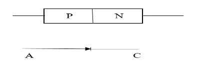
Current conventionally flows in the direction indicated by the arrow (A to C) while it is not allowed in the reverse direction. A P-N junction diode offers minimal resistance in forward bias and behaves like an insulator in reverse bias hence mostly used to rectify ac current to dc current.
Voltage-Current Characteristics
Forward Characteristic
When an external voltage is applied from zero in an increasing manner and in forward direction, no current flows through the device initially. This is due to the availability of an internal voltage Vb=0.7V in Si and 0.3V in Ge, which opposes the applied voltage for some time until is neutralized to eventually allow rapid increase of current through the diode
Reverse Characteristic
In reverse bias mode, only a small current due to minority charge carriers is allowed through while current due to majority carriers is locked out. Saturation current I0 also known as leakage current is reached quickly with increasing external voltage from zero value. This saturation current is dependent to temperature, junction size and doping degree as opposed to the applied external voltage. When the reverse voltage supersedes the breakdown voltage Vbr, a sharp increase is experienced in the leakage current with negligible resistance at this point. Any further additional voltage may cause burning out of the diode unless it is protected by a resistor as a current limiter.
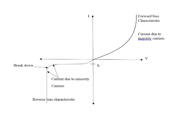
Reverse bias characteristic
The Zener diode is used in voltage stabilizing circuits. It is usually operated in reverse bias where it undergoes Zener breakdown, which occurs in heavily doped junctions with narrow depletion layers. The diode power dissipation and external resistance limit current in the breakdown region. Zener breakdown occurs within voltages less than 6V, beyond which Avalanche breakdown predominates. Strong electric fields up to 108V/m are formed during this kind of breakdown. The set up field is usually strong enough to destroy covalent bonds resulting to electron-hole pairs, and any small increase in reverse voltage may result to massive increase in carrier numbers, hence low resistance at the junction in the breakdown region.
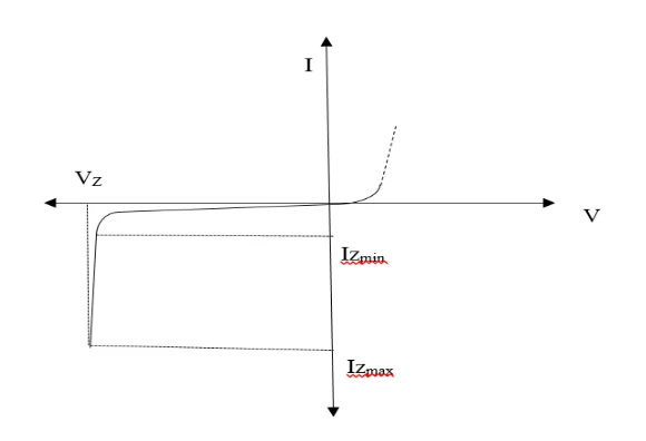
Voltage-Current Characteristics
VZ=Zener breakdown voltage
Izmin=Minimum current required for breakdown to occur
Izmax=Maximum current usually limited by maximum power dissipation.
Transistor works as a switch in saturation and cutoff regions. Collector-base and emitter-base junctions are reverse biased in cutoff state while both are forward biased in saturation region. It can also be said that transistor allows current passage through collector-emitter track only when the base is supplied with voltage. Switch is ON when there is a base voltage and vise versa. Emitter is connected to the ground of the circuit while the collector is connected to the load to be switched on by the transistor.
In cut-off region;
Input and base are grounded
Base-emitter VBE voltage is less than 0.7V
Base-emitter junction is reverse biased
Consequently
Transistor is completely OFF
Collector current IC=0
Vout=VCE=VCC=1
Transistor is a switch in an open position.
In saturation position;
Input and base are linked to VCC
Base-emitter voltage VBE is greater than 0.7V
Forward biased base-emitter junction
Consequently;
Transistor is completely ON
Collector current is maximum. IC=VCC/RL
VCE=0
Transistor is a closed switch.
Rectifier Diode- this is a semiconductor device with two leads that allow current to pass in only one direction. It is used in power supply equipment to convert alternating current (AC) to direct current (DC). The simplest rectifier circuit is the half-wave rectifier, which allows passage of only one half of the AC waveform. Full wave rectification allows full use of both cycles of ac AC sinusoidal signal. Also used as radio signal detector.
Thyristor- this is a four layer solid state semiconductor device with alternating P type and N type layers. It is used as a bistable switch, which is triggered to conduct when the base is connected to a current source. The device continues to conduct until it is either reverse biased or the trigger voltage is removed. It is usually applied in high voltage and current circuits. It is also used in phase fired controllers as the control element.
DIAC- in full it is the diode for alternating current, which only conducts after a certain voltage has been attained. This is called the DIAC breakover voltage VBO. A DIAC is a semiconductor switch with bidirectional properties hence can conduct in both forward and reverse properties. It is used to establish distinct switching for a TRIAC.
TRIAC- this stands for triode for alternating current, which is a bidirectional three terminal device that conducts in either forward or reverse direction when triggered. Technically, it is referred to as the bilateral triode thyristor or bidirectional triode thyristor. It is usually a current driven device which is self-sustaining, meaning it remains conducting once turned on until the current is reversed. TRIACs are used in medium power AC switching and can switch the two halves of AC cycle. They are also ideal for power control applications.
Light Emitting Diode- commonly referred to as LED. This is a semiconductor device with p-n junction that emits light when current passes through it. During this process, energy is released in form of photons due to recombining of electrons with electron holes. It is mainly used for lighting purposes.
Bipolar Junction Transistors (BJTs)
This is basically a semiconductor device comprising two back-to-back P-N junctions combined on common semiconductor crystal. The P-N junctions result in three transistor regions including:
Emitter- Mainly supplies the majority charge carriers to the base hence is usually the most heavily doped. The majority charge carriers may either be electrons or holes.
Base- Is usually the very thin middle section of the transistor. It is the least doped of the three regions.
Collector- As the name suggests, it collects majority charge carriers from emitter and channels them to the base. The collector is thus made physically bigger since it dissipates more power.
BJT can either be a P-N-P or N-P-N type depending on its manufacturing architecture. They are mainly used as electric signal boosters in linear amplifiers.
They are also used as electronic switches.

Field Effect Transistors (FETs)
These are unipolar solid state three terminal semiconductor devices. Just like in vacuum tubes, current in FET devices is controlled by electric field. FETs are of two types:
Junction Field Effect Transistor (JFET)
Fabricated as either P channel or N channel with preference to N channel. To make an N channel JFET, a narrow N type semiconductor is sandwiched and diffused with P type junctions to form two P-N gates with the channel in between these gates. Electrical connections are done at the source (S) and drain (D) terminals and majority charge carriers are the electrons. P channel JFET is fabricated in a similar way only that two N type junctions are used with one P type bar.
Source- Majority charge carriers come from it hence the name. Majority charge carriers enter the bar through this terminal.
Drain- Majority charge carriers leave the bar through this terminal.
Gate- these are two impurity regions that are heavily doped and internally connected to form two P-N junctions.
Channel- Passage through which majority charge carriers flow from source to drain.
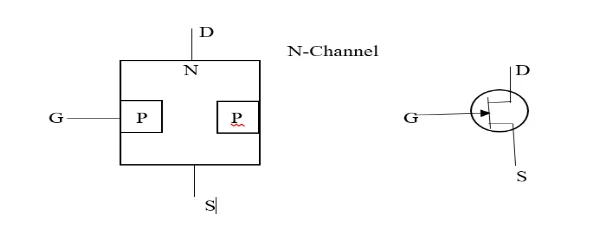
N-channel Diode
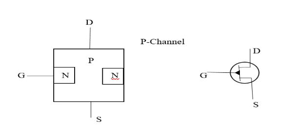
P-channel diode
Metal Oxide Field Effect Transistors (MOSFETs)
These are further sub-divided into:
Depletion enhancement MOSFET (DE MOSFET): Changing polarity of VGS allows operation in both depletion and enhancement modes.
Enhancement only MOSFET- Only works with large positive gate voltages, and operates in enhancement mode only.
TASK 4
Analogue system is a way of representing numerical values of a physical quantity in a continuous manner. For instant, an oven`s temperature can be set to any value between 00 and 1000. i.e. this value may be 560, 56.670, 56.6790,56.67910 etc. Current through a certain component in a circuit may also be measured as a continuous physical quantity say 2.5A, 2.51A, 2.515A etc. The figures may simply go continuously all the way to infinity.
On the other hand, digital systems involve discrete or step by step representation of numerical values of physical quantities. They mostly involve representation of values using binaries. Eg the oven temperature may be set as 560, 570, 580 etc. thus increasing in steps of 10.
Amplifier Gain
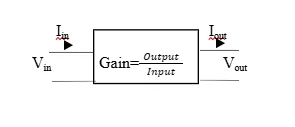
This is simply the measure of an amplifier`s ability to amplify an input signal. Amplifier gain can be measured using three possible quantities:
Voltage gain (AV) = Output voltage/Input voltage
Current gain (AI) = Output current/Input current
Power gain (AP) = Output power/Input power = AV X AI
Ideal operational amplifiers usually have infinite open loop gain, which remains constant for varying input values.
Amplifier band width
This is the range of frequencies over which an amplifier`s voltage gain is above 70.7 % or -3dB. The maximum output value is usually 0dB. This range of frequencies usually decreases with increase in amplifier gain. An ideal operational amplifier has an ideal gain resulting to infinite band width.
Amplifier input
This is the impedance seen by the driving source. Ideal operational amplifiers have infinite input impedance. This impedance may vary according to supply source.
Amplifier output
Ideal operational amplifiers have zero output impedance. This impedance may vary with load impedance connected across the output terminals.Op amps have infinite output voltage range.
Amplifier distortion
This usually occurs in non-linear amplifiers, which may experience time delay between input and output signals. Harmonic distortion may occur due to under voltage of the power supply connected to the amplifier. Ideal amplifiers have minimum distortion in the audio frequency range.
Let the input variables be A and B respectively. The first set of two logic gates invert the inputs separately. i.e.
F=A-1 and F=B-1 respectively.
The second set consists of one logic gate at the center of the circuit, which combines the inverted variables the further inverts the output. Thus,

F=( A-1+ B-1)-1=AB
The last logic gate then inverts the combined variables to attain the overall output. Therefore,
F=(AB)-1
Truth Table
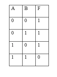
The combinational logic gate yields the NAND function.
Analogue meters: can display any numerical value within its scale for physical quantities.
Digital meters: can only display discrete values for physical quantities they measure.
Light dependent resistor (LDR): this is a light sensor which depends on light intensity for its performance. Its resistance varies with light intensity. It is analogue in nature.
Audio amplifiers: this an analogue system that gives an output voltage of any value within the range of the input.
Microphones: accepts any value of audio signal within the range of it supply. This is an analogue system.
Compact disc (CD): records and convers sound into digital form.
- 24/7 Customer Support
- 100% Customer Satisfaction
- No Privacy Violation
- Quick Services
- Subject Experts


